
Electronics & advanced materials

Powder, paste, ceramic, carbon, optical, and recovered-material behavior across electronics production

Semiconductor precursors, conductive metals, dielectric ceramics, functional inks and recovered streams are not
one category

Purity, particle size, oxidation, surface chemistry, agglomeration, electrostatics, dispersion,
and rheology decide whether electronics materials dose consistently, form uniform layers,
print and coat cleanly, polish without defects, and deliver the conductivity, dielectric response,
thermal performance or optical properties required. This page connects what you are seeing in
production to the mechanism behind it and the measurement that helps separate the likely causes.

Icon representing electronics and advanced-material routes

By material type

Semiconductors, conductive metals, dielectric ceramics, ferrites, thermal materials, carbons, inks, optical powders and recovered streams.

Icon representing recurring powder behavior routes

By observed behavior

Flow, caking, dust, dosing, agglomeration, segregation, contamination, moisture, oxygen sensitivity, dispersion and printing instability.

Icon representing powder measurement routes

By measurement route

Separate likely mechanisms with particle, bulk, surface, moisture, composition, electrostatic, dispersion and thermal measurements.

Icon representing process area routes

By process area

Purification, milling, storage, dosing, mixing, printing, coating, drying, curing, sintering, polishing, recovery and recycling.

Find your route

Start with the material, then the behavior

Electronics and advanced materials do not behave as one category. Pick the semiconductor, conductive, dielectric, magnetic, thermal, carbon, encapsulant, ink, optical, abrasive or recovered-material class, then the behavior you are seeing in the process. The result names the routes worth checking next. It is a triage route, not a diagnosis.

  1. 1Material
  2. 2Behavior
  3. 3Route

Step 1  What are you handling?

Step 2  What are you seeing?

Step 3  Your route

Material routes

Semiconductor, conductive, dielectric, magnetic, optical, and recovered streams

Electronics production handles high-purity semiconductor precursors, metallic conductors, dielectric and magnetic ceramics, thermally conductive fillers, nanoscale carbons, filled encapsulants, functional inks, optical powders, polishing abrasives, and recovered streams with very different particle sizes, densities, surface chemistries, atmosphere sensitivities, electrostatic behaviors, and rheological responses. Each class has its own behavior profile, so the most useful route starts with the material before moving to the visible symptom or process instability. For semiconductor-specific handling, purity and process routes, continue to <a href=”/industries/semiconductors/”>Semiconductor Materials</a>.

Semiconductor silicon feedstock material in a shallow stainless steel sample dish

Semiconductor silicon feedstock materials

Semiconductor silicon feedstocks require extreme purity and controlled surfaces. Particle size, oxygen, metallic traces, and handling affect growth, deposition, and yield.

Purity Surface Yield
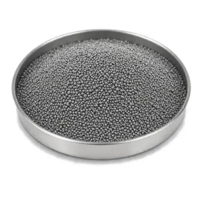
Compound semiconductor feedstock in a shallow stainless steel sample dish

Compound semiconductor feedstocks

Compound semiconductor materials require precise stoichiometry and purity. Oxidation, moisture, particle size, and contamination directly affect growth, deposition, and performance.
Stoichiometry Purity Growth
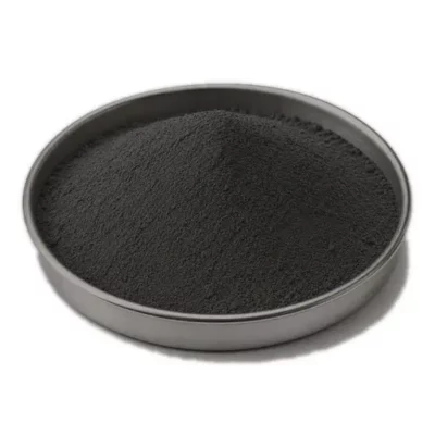
Conductive metal powder and paste material in a shallow stainless steel sample dish

Conductive metal powders and pastes

Silver, copper, and nickel powders must disperse and sinter consistently. Size, shape, oxidation, solids loading, and rheology affect printing and conductivity.
Mixing Sintering Conductivity
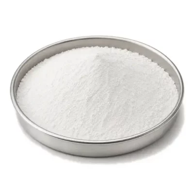
Dielectric and capacitor ceramic powder in a shallow stainless steel sample dish

Dielectric and capacitor ceramic powders

Dielectric ceramic powders require controlled size, dopants, and surface area. Agglomeration, packing, and contamination affect layer formation, sintering, and permittivity.
Dopants Packing Permittivity
Ferrite and magnetic powder material in a shallow stainless steel sample dish

Ferrites and magnetic powder materials

Ferrite and magnetic powders depend on composition, oxidation state, and particle structure. Granulation, packing, and sintering influence density and magnetic losses.
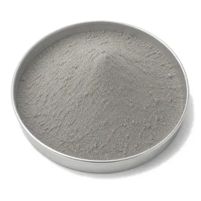
Composition Firing Magnetics
Thermal-management ceramic material in a shallow stainless steel sample dish

Thermal-management ceramic materials

Aluminum nitride, boron nitride, and related ceramics require controlled surfaces and packing. Moisture, oxygen, and dispersion affect processing and thermal conductivity.
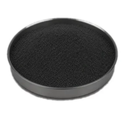
Surface Packing Conductivity
Graphene nanotube and conductive carbon material in a shallow stainless steel sample dish

Graphene, nanotubes, and conductive carbons

Conductive carbons are low-density, cohesive, and difficult to disperse. Agglomeration, dust, electrostatics, and dosing variation affect networks and conductivity.
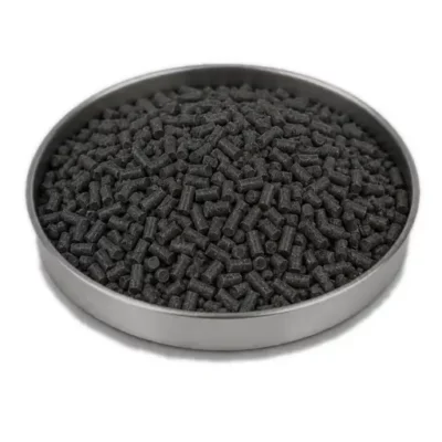
Mixing Networks Conductivity
Electronic encapsulant and mold compound in a shallow stainless steel sample dish

Electronic encapsulants and mold compounds

Encapsulants combine resin, silica filler, pigments, and additives. Filler distribution, moisture, flow, and cure behavior directly affect molding, voids, stress, and reliability.
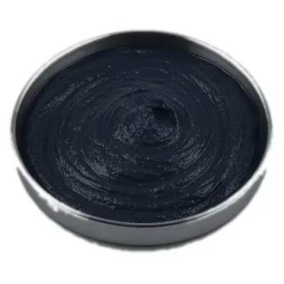
Filler Molding Reliability
Printed-electronics ink and coating material in a shallow stainless steel sample dish

Printed-electronics inks and coatings

Functional inks require stable particle dispersion, wetting, and rheology. Solids loading, evaporation, agglomeration, and surface chemistry directly affect overall printing consistency and curing.
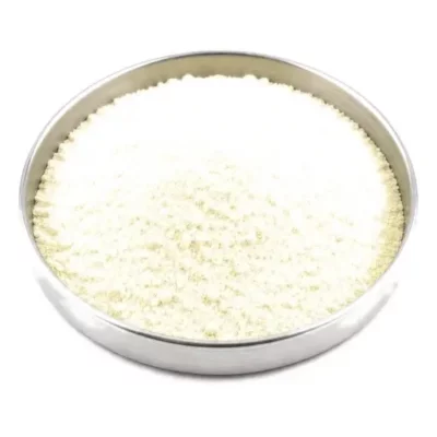
Rheology Printing Curing
Optical and luminescent powder material in a shallow stainless steel sample dish

Optical and luminescent materials

Optical and phosphor powders require controlled size, morphology, dopants, and coatings. Agglomeration, moisture, and contamination affect dispersion, color, and brightness.
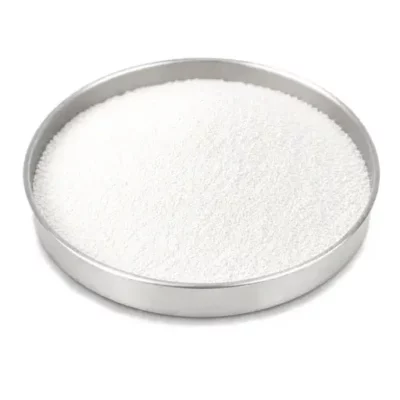
Dopants Dispersion Brightness
CMP abrasive and polishing powder in a shallow stainless steel sample dish

CMP abrasives and polishing powders

CMP abrasives require tightly controlled size and slurry stability. Agglomerates, oversized particles, chemistry, and contamination directly affect material removal, surface scratches, and processing defects.
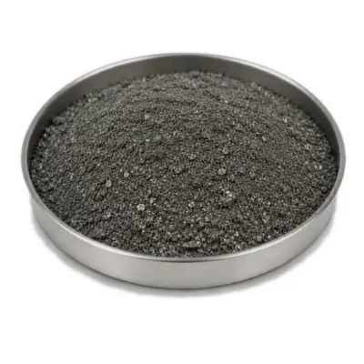
Size control Polishing Defects
Recovered electronic material stream in a shallow stainless steel sample dish

Recovered electronic material streams

Recovered electronic streams contain mixed metals, ceramics, carbons, and residues. Liberation, contamination, oxidation, and size distribution affect sorting and recovery.

Liberation Sorting Recovery

Quick comparison

Material route, common risk, first measurement

Quick comparison The same symptom can point to different mechanisms depending on the material class, particle size, purity requirement, surface chemistry, atmosphere, formulation, and thermal route. Use this comparison as a fast bridge between electronics-material behavior and the most useful first measurement route.

Electronics and advanced-material routes, the handling or processing risk each one carries most often, and the measurement worth running first.

Material routeCommon handling or processing riskUseful first measurement
Semiconductor silicon feedstock materialsMetallic contamination, oxidation, surface change, and inconsistent growth or depositionParticle size, oxygen, metallic impurities, and surface condition
Compound semiconductor feedstocksStoichiometric drift, oxidation, moisture, contamination, and unstable crystal growthComposition, purity, oxygen, and particle size
Conductive metal powders and pastesOxidation, agglomeration, unstable rheology, poor printing, and conductivity variationParticle size, morphology, solids loading, and rheology
Dielectric and capacitor ceramic powdersAgglomeration, dopant variation, poor packing, and inconsistent dielectric responseParticle size, surface area, dopant distribution, and density
Ferrites and magnetic powder materialsComposition drift, oxidation, granule variation, and inconsistent magnetic performanceComposition, particle size, oxidation state, and bulk density
Thermal-management ceramic materialsMoisture sensitivity, oxygen pickup, poor dispersion, and reduced thermal conductivityMoisture, oxygen, particle size, and surface condition
Graphene, nanotubes, and conductive carbonsExtreme cohesion, dust release, electrostatics, and poor conductive-network formationBulk density, electrostatics, wetting, and dispersion
Electronic encapsulants and mold compoundsFiller segregation, moisture, unstable flow, voids, and cure-related stressFiller distribution, moisture, flowability, and cure response
Printed-electronics inks and coatingsSettling, agglomeration, viscosity drift, poor wetting, and printing defectsParticle size, dispersion stability, rheology, and wetting
Optical and luminescent materialsAgglomeration, dopant or coating variation, contamination, and inconsistent brightnessParticle size, morphology, composition, and dispersion
CMP abrasives and polishing powdersOversized particles, agglomeration, contamination, scratches, and removal-rate variationParticle-size tails, agglomerates, chemistry, and contamination
Recovered electronic material streamsMixed composition, contamination, oxidation, poor liberation, and recovery variationComposition, particle size, liberation, and contamination screening

Recurring problems

Start from the behavior you can see

Start from the behavior you see in the process. These routes connect common electronics and advanced-material symptoms to likely mechanisms, material sensitivities, process areas, and useful measurement routes.

Icon representing poor flow and discharge

Poor flow

Arching · Bridging · Discharge

Icon representing caking or hardening

Caking or hardening

Moisture · Load · Storage

Icon representing dust and nanoparticle release

Dust and nanoparticle release

Fines · Exposure · Containment

Icon representing dosing and formulation variation

Dosing and formulation variation

Density · Feeding · Variation

Icon representing segregation

Agglomeration or segregation

Size · Density · Mixing

Icon representing contamination or equipment wear

Contamination or equipment wear

Purity · Wear · Recovery

Icon representing moisture oxygen and atmosphere sensitivity

Moisture & atmosphere sensitivity

Moisture · Oxygen · Surface

Icon representing printing coating and thermal instability

Printing & coating instability

Print · Cure · Performance

Measurement routes

The test that answers your question

Electronics-material behavior often requires more than one measurement. Particle size, morphology, purity, moisture, oxygen, cohesion, electrostatics, density, surface area, rheology, dispersion, contamination, and thermal response can all contribute to the same visible process symptom.

Particle size and morphology

Particle size distribution
Fines, oversize, agglomerates, packing, milling endpoint, granule size, melting, and forming consistency.

Microscopy and morphology
Shape, angularity, platelets, granule structure, fracture, surface texture, and packing or rheology response.

Moisture, oxygen, and surface condition

Moisture and environmental response
Free moisture, bound water, hygroscopicity, storage history, caking, plasticity, and drying response.

Surface and thermal response
Organics, carbonates, hydroxyls, surface treatments, binder interaction, firing gases, and wetting response.

Flowability, packing, and electrostatics

Powder flow and bulk mechanics
Cohesion, consolidation, hopper discharge, batching, die filling, granule flow, and transfer stability.

Density, packing and aeration
Packing, aeration, settling, compaction, fill consistency, porosity, and batch-volume control.

Composition, density, and segregation behavior

Composition and contamination
Airborne fines, cross-contamination, size or density separation, material loss, and housekeeping.

Density, porosity and surface area
Open and closed porosity, specific surface area, pore structure, binder demand, sintering, and absorption.

Dispersion, rheology, and thermal response

Dispersion and rheology
Solids loading, viscosity, yield stress, thixotropy, settling, casting, coating, and drying stability.

Thermal and solid-state response
Drying, binder burnout, decomposition, phase change, sintering, melting, crystallization, and process-window sensitivity.

Process routes

Where material behavior appears in electronics production

The same electronics material can behave differently depending on where it is in the process. Purification, milling, storage, dosing, mixing, dispersion, printing, coating, drying, curing, sintering, polishing, and recovery each expose different material properties and failure mechanisms. For equipment-specific routes, see Conveying & Transfer and Feeding & Dosing.

01

Purification and preparation

Refining, precipitation, calcining, drying, screening, and atmosphere control determine purity, composition, surface condition, and later process consistency.

02

Milling and classification

Mill type, energy input, classifier settings, particle hardness, morphology, and agglomeration influence fines, oversize, surface area, and usable yield.

03

Storage atmosphere control

Humidity, oxygen, consolidation, packaging, reclaim sequence, and exposure time can alter caking, oxidation, surface chemistry, and composition.

04

Conveying and precision dosing

Bulk density, cohesion, aeration, electrostatics, feeder design, and refill strategy influence discharge, dosing stability, and formulation delivery.

05

Mixing, blending, and dispersion

Particle size, density, surface chemistry, solids loading, mixing energy, and addition sequence influence agglomeration, additive distribution, and uniformity.

06

Printing, coating, and deposition

Wetting, rheology, particle size, layer thickness, substrate condition, and deposition settings influence coverage, defects, adhesion, and electrical performance.

07

Drying, curing, and debinding

Solvent removal, heating rate, binder chemistry, gas release, permeability, and atmosphere influence cracking, blistering, residue, and dimensional stability.

08

Sintering and thermal treatment

Atmosphere, temperature profile, particle contacts, phase changes, oxidation, and heat transfer influence densification, conductivity, color, and reliability.

09

Material recovery and recycling

Liberation, screening, sorting, contamination control, blending, and reuse limits determine recovered-material consistency, yield, and final quality.

Go deeper

Guides and articles for electronics and advanced materials

Published technical articles that go further into conductive powders, electronic feedstocks and the particle-level mechanisms behind electrical performance.
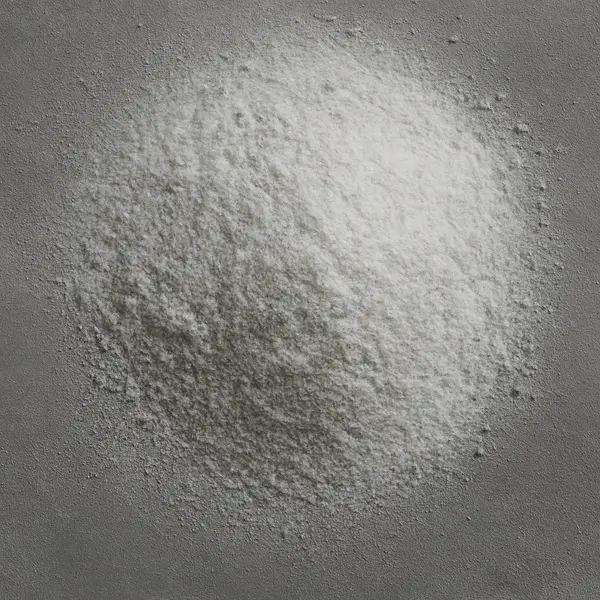
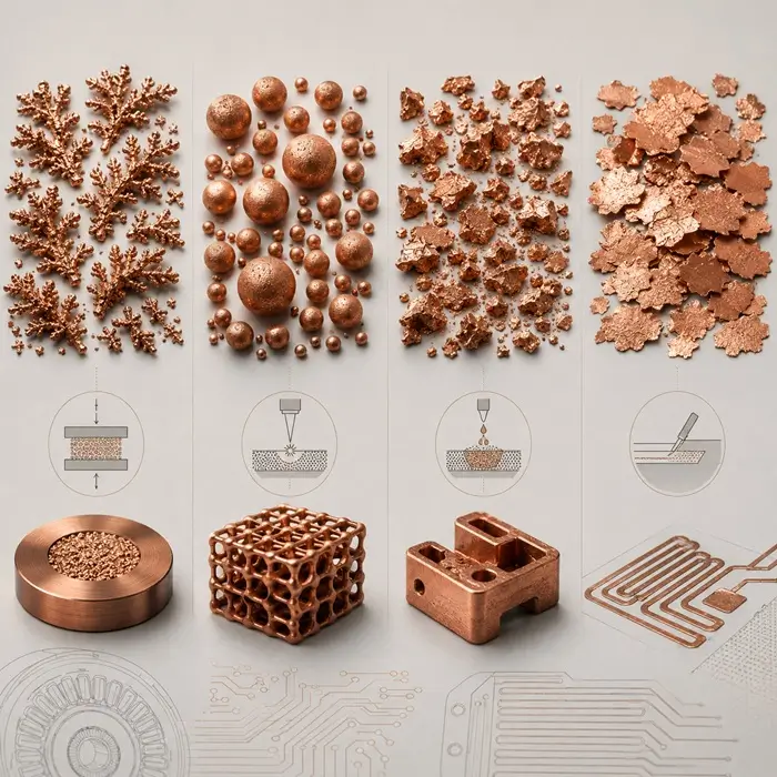
Powder-based electronics materials and printed electronic structures

The Future of Powder-Based Electronics: Enabling New Possibilities

How powder behavior, quality control and processing increasingly shape printed electronics, sintered interconnects and other electronic manufacturing routes.

Copper powder used in electrification and conductive applications

Copper Powder for Electrification: Why Morphology, Purity, and Packing Density Are Now Engineering Variables

Why morphology, particle size, purity, packing density and surface chemistry have to match the actual conductive application rather than a generic copper-powder specification.

Conductive particle network in a composite feedstock

Powder Percolation Threshold and Conductive Networks in Composite Feedstocks

Why small changes in dispersion, drying, shear or oxide growth can strongly change conductivity when a formulation sits close to the percolation threshold.

Define practical electronics process windows

Connect poor flow symptoms to cohesion, wall friction, consolidation, aeration, electrostatics, hopper geometry, feeder interaction and likely precision-dosing limitations.

Packing, coating and uniformity

Review particle size, morphology, density, electrostatics, coating conditions and layer thickness when segregation, streaking, voids or uneven deposition appears.

Dispersion and rheology control

Link solids loading, particle size, surface chemistry, dispersant level, viscosity, yield stress, wetting, air and drying history to printing, coating, settling and defects.

FAQ

Electronics and advanced materials questions

Similar symptoms can result from cohesion, particle morphology, moisture, oxygen, electrostatics, agglomeration, segregation, contamination, density differences, rheology, or interaction between the material and equipment.
Material behavior depends on the conditions acting on it. Storage history, atmosphere, consolidation, moisture, mixing energy, shear, coating thickness, drying rate, temperature, and residence time can shift how the same material feeds, disperses, prints, coats, cures, sinters, or polishes.
The useful method depends on the question. Particle-size and morphology analysis may help with flow, packing, coating, or segregation, while moisture, oxygen, surface area, density, electrostatics, rheology, dispersion, thermal analysis, composition, or contamination screening may be more relevant for other symptoms.
Start with the information you already have. Use the material route when the material class is known, the behavior route when a visible symptom drives the investigation, and the measurement route when you already know which property or test family needs evaluation.
Laboratory testing is useful when the symptom does not reveal the controlling mechanism, when several causes are plausible, or when a new raw material, formulation, process setting, or reuse strategy needs evaluation before implementation. Test conditions should reproduce the relevant atmosphere, stress, temperature, shear, and handling history.
Yes. Unstable feeding, poor dispersion, coating variation, printing defects, cure failure, sintering inconsistency, scratches, or electrical variation can result from several interacting factors. Complementary measurements can help separate effects such as particle size, morphology, moisture, oxygen, cohesion, density, surface chemistry, rheology, contamination, and process history.

Need the measurement, not just the guidance? PowderTechnology.info works closely with Delft Solids Solutions,
a contract research organization specializing in the physical behavior of powders and granules. DSS provides
contract testing and characterization, with its laboratory working in accordance with ISO 17025.
Contact Delft Solids Solutions.

Delft Solids Solutions logo