
Semiconductor materials
High-purity feedstock, slurry, precursor and packaging-material behavior across semiconductor manufacturing
Silicon, compound semiconductors, precursors, lithography materials, CMP slurries, dielectrics, interconnects and packaging compounds are not one category
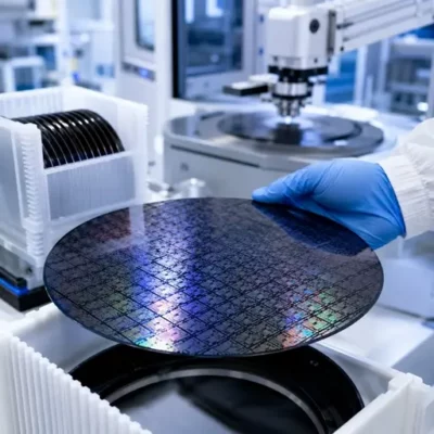
Purity, particle-size tails, oxygen, moisture, surface chemistry, agglomeration, electrostatics, rheology and contamination decide whether semiconductor materials deliver consistently, deposit cleanly, pattern uniformly, polish without scratches, and meet wafer-yield and reliability requirements. This page connects the process symptom or wafer defect to the mechanisms worth separating and the measurement that helps identify the likely cause.
Semiconductor materials
High-purity feedstock, slurry, precursor and packaging-material behavior across semiconductor manufacturing
Silicon, compound semiconductors, precursors, lithography materials, CMP slurries, dielectrics, interconnects and packaging compounds are not one category
Purity, particle-size tails, oxygen, moisture, surface chemistry, agglomeration, electrostatics,
rheology and contamination decide whether semiconductor materials deliver consistently,
deposit cleanly, pattern uniformly, polish without scratches, and meet wafer-yield and
reliability requirements. This page connects the process symptom or wafer defect to the
mechanisms worth separating and the measurement that helps identify the likely cause.



Find your route
Start with the material, then the behavior
Semiconductor materials do not behave as one category. Pick the silicon, compound semiconductor, dopant, precursor, lithography, CMP, dielectric, interconnect, packaging or recovered-material class first, then choose the behavior or process instability you are seeing. The result identifies the mechanisms worth separating, the measurement to start with and where in the process the issue usually appears. It is a triage route, not a diagnosis.
- 1Material
- 2Behavior
- 3Route
Step 1 What are you handling?
Step 2 What are you seeing?
Step 3 Your route
Material routes
Silicon, compound semiconductors, process chemicals, slurries and packaging materials
Semiconductor manufacturing handles electronic-grade silicon, wide-bandgap and compound semiconductor sources, dopants, deposition materials, lithography formulations, CMP abrasives, dielectric materials, interconnect metals, thermally conductive fillers, encapsulants and reclaimed process streams with very different purity requirements, particle sizes, surface chemistries, atmosphere sensitivities, electrostatic behaviors and rheological responses. Each class has its own behavior profile, so the most useful route starts with the material before moving to the visible defect or process instability.

Electronic-grade silicon and polysilicon
Electronic-grade silicon and polysilicon require extreme purity and controlled surfaces. Particle size, oxygen, metallic traces, and handling influence growth and yield.

Silicon carbide semiconductor materials
Silicon carbide materials require controlled polytype, purity, and surface condition. Particle size, oxygen, contamination, and handling affect crystal growth and wafer quality.

GaN and compound semiconductor materials
GaN and related compound semiconductors require precise stoichiometry and purity. Moisture, oxidation, particle size, and contamination affect growth and performance.

Dopant sources and diffusion materials
Dopant sources require controlled composition, purity, and delivery. Moisture, particle size, volatility, and contamination affect diffusion, activation, and uniformity.

Deposition precursors and source materials
Deposition sources require stable composition, purity, and delivery. Moisture, agglomeration, volatility, and residue influence film growth and chamber stability.

Photoresists and lithography materials
Lithography materials require dispersion, filtration, wetting, and viscosity. Particles, agglomerates, moisture, and aging affect coating, patterning, and defects.

CMP abrasives and polishing slurries
CMP materials require tightly controlled particles, chemistry, and slurry stability. Agglomerates, oversized particles, and contamination affect removal, scratches, and defects.

Dielectric and insulating materials
Dielectric materials require controlled purity, particle size, and surface chemistry. Agglomeration, moisture, and contamination affect deposition, cure, and insulation.

Conductive metals and interconnect materials
Copper, tungsten, cobalt, and related materials require purity and controlled deposition. Oxidation, particles, and residues affect resistance and reliability.

Thermal-interface and packaging materials
Thermal-interface materials combine conductive fillers with polymers or binders. Filler packing, dispersion, moisture, and flow affect heat transfer and assembly.

Encapsulants, underfills, and mold compounds
Encapsulants and underfills combine resin, silica filler, and additives. Filler distribution, moisture, flow, and cure behavior affect voids, stress, and reliability.

Reclaimed wafer and process material streams
Reclaimed streams contain silicon, metals, ceramics, abrasives, residues. Liberation, contamination, oxidation, and size affect sorting and recovery.
Quick comparison
Material route, common risk, first measurement
The same symptom can point to different mechanisms depending on the material class, purity requirement, particle-size tail, surface chemistry, atmosphere, formulation and process step. Use this comparison as a fast bridge between semiconductor-material behavior and the most useful first measurement route.
Semiconductor material routes, the handling or process risk each one carries most often, and the measurement worth running first.
| Material route | Common handling or processing risk | Useful first measurement |
|---|---|---|
| Electronic-grade silicon and polysilicon | Metallic contamination, oxidation, surface change, and inconsistent crystal growth | Particle size, oxygen, metallic impurities, and surface condition |
| Silicon carbide semiconductor materials | Polytype variation, oxygen, contamination, crystal defects, and wafer-quality variation | Composition, oxygen, particle size, and surface condition |
| GaN and compound semiconductor materials | Stoichiometric drift, oxidation, moisture, contamination, and unstable growth | Composition, purity, oxygen, and particle size |
| Dopant sources and diffusion materials | Composition drift, moisture, unstable delivery, contamination, and non-uniform activation | Composition, moisture, particle size, and contamination |
| Deposition precursors and source materials | Moisture uptake, agglomeration, residue, unstable delivery, and film defects | Purity, moisture, particle size, and residue analysis |
| Photoresists and lithography materials | Particles, agglomerates, viscosity drift, poor wetting, and pattern defects | Particle contamination, filtration, rheology, and wetting |
| CMP abrasives and polishing slurries | Oversized particles, agglomeration, contamination, scratches, and removal-rate variation | Particle-size tails, agglomerates, chemistry, and contamination |
| Dielectric and insulating materials | Agglomeration, moisture, contamination, coating defects, and insulation variation | Particle size, moisture, surface chemistry, and purity |
| Conductive metals and interconnect materials | Oxidation, particles, residue, poor deposition, and resistance variation | Purity, oxygen, particle size, and contamination |
| Thermal-interface and packaging materials | Filler segregation, poor dispersion, voids, unstable flow, and heat-transfer variation | Filler distribution, rheology, moisture, and thermal conductivity |
| Encapsulants, underfills, and mold compounds | Filler segregation, moisture, voids, cure variation, and package stress | Filler distribution, moisture, flowability, and cure response |
| Reclaimed wafer and process material streams | Mixed composition, contamination, oxidation, poor liberation, and recovery variation | Composition, particle size, liberation, and contamination screening |
One risk per row is the one most often reported, not the only one that occurs. Use the selector above to work a specific material and process symptom through to a route.
Recurring problems
Start from the behavior you can see
These eight routes connect common semiconductor-material and wafer-process symptoms to likely mechanisms, material sensitivities, process areas and useful measurements.




Also covered: electrostatic charging, adhesion and fouling, and wetting and dispersion. All symptoms
Measurement routes
The test that answers your semiconductor process question
Semiconductor-material behavior often requires more than one measurement. Particle size, morphology, purity, moisture, oxygen, surface chemistry, cohesion, electrostatics, density, rheology, dispersion, contamination and thermal response can all contribute to the same visible process symptom or wafer defect.
Compare every method All test methods on the site, grouped by the question they answer.
Process routes
Where material behavior appears in semiconductor manufacturing
The same semiconductor material can behave differently depending on where it is in the process. Purification, crystal growth, wafer preparation, deposition, doping, lithography, etching, cleaning, CMP, packaging and recovery each expose different material properties, contamination pathways and failure mechanisms.
Go deeper
Guides and articles for semiconductor materials
Longer reads that work through semiconductor materials and processes, from particles and surfaces to deposition, patterning, polishing and recovery.


FAQ
Semiconductor material questions
Need the measurement, not just the guidance? Semiconductor-material problems often cannot be explained by one measurement alone. A delivery problem may involve cohesion, density, electrostatics, moisture, carrier gas, hopper geometry or feeder interaction. Crystal-growth, deposition, lithography, CMP, cleaning, packaging and reliability problems can involve particle-size tails, purity, surface chemistry, dispersion, rheology, contamination, atmosphere or process history. PowderTechnology.info works closely with Delft Solids Solutions for contract testing and interpretation. Contact Delft Solids Solutions.