
Powder-based electronics are no longer just a research curiosity. Today, they actively reshape how we design and manufacture next-generation devices. From printable circuits to sintered interconnects, powder technologies now drive innovation across electronics manufacturing.
In this article, we explore the latest developments, examine the materials currently in use, and address key practical challenges. Along the way, R&D and QC professionals will gain a clear, actionable view of where the field is heading—and how to prepare for what comes next.
Printed Electronics: Powders That Conduct and Compute
One of the most dynamic areas in powder-based electronics is printed electronics, which uses conductive inks and semiconducting powders to build functional components. Manufacturers print these materials directly onto substrates using methods like inkjet, screen, or aerosol printing.
Currently, silver nanoparticle inks lead the field thanks to their excellent conductivity and low curing temperatures. However, rising costs and sustainability concerns are pushing researchers and industry to explore alternatives. Copper nanoparticle inks, for example, are gaining momentum. Thanks to recent advancements in ink formulation, copper can now be laser-sintered in air—minimizing oxidation and eliminating the need for inert atmospheres.
At the same time, semiconducting powders—including organic semiconductors and metal oxides—have also become printable. These materials make it possible to fabricate thin-film transistors and sensors without relying on traditional lithographic techniques.
In research labs, scientists have already printed complete circuits using layered powder-based materials, including diodes, transistors, and sensors. Now, industrial interest is accelerating, especially for applications like flexible displays, smart labels, and low-power IoT devices.
Sintered Powder Components: High-Performance Bonds and Layers
Sintered powders are already transforming component design in high-power and high-frequency electronics. In electric vehicles, for example, sintered silver is used for die attach and interconnects. It offers thermal conductivity over 200 W/m·K—far better than conventional solders.
These pastes, made from nano or micron-scale silver particles, sinter at low pressure and moderate temperatures. As a result, they enable more reliable, high-performance bonding in power modules.
The next frontier is sintered copper, which is more affordable but trickier to process. Copper particles oxidize easily, which limits conductivity and bonding. New formulations—like copper-silver hybrids or coated copper flakes—are addressing this. These solutions allow sintering in ambient air, expanding the technology’s industrial potential.
Beyond interconnects, powder sintering is used for ceramic capacitors, magnetic cores, and RF components, where precision layering of dielectric and metallic powders creates compact, high-functionality elements.
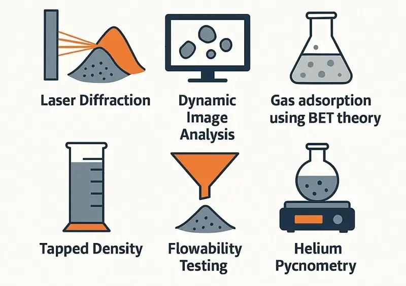
Powder Quality and Processing: Where QC Must Step In
Whether printing or sintering, powder quality is critical. For R&D teams, the focus is on formulating stable, repeatable processes. For QC managers, the challenge lies in verifying consistency batch after batch.
Key concerns include:
-
Particle morphology: Spherical particles flow and print better, while flakes may offer higher conductivity but worse dispersion.
-
Oxidation control: For copper-based powders, oxidation degrades performance. Monitoring oxide thickness is essential.
-
Ink rheology: Inks must maintain uniformity during printing. Settling or agglomeration leads to defects.
-
Curing and sintering: Time, temperature, and environment impact final properties. Real-time monitoring helps catch anomalies early.
In sintering, voids, porosity, and uneven bonding can undermine reliability. Inline inspection tools—like X-ray imaging and resistivity mapping—are increasingly used to validate outcomes.
A stable process depends not just on good materials, but on tight process control, feedback systems, and traceable quality standards.
Early Adoption: Where Powder-Based Electronics Are Taking Off
Commercial adoption is underway, especially where form factor, cost, or customization offer a competitive edge. Notable applications include:
-
Wearables: Printed sensors embedded in textiles or skin patches for health monitoring.
-
Smart packaging: Labels that indicate freshness or log environmental exposure.
-
Automotive electronics: Sintered silver joints in EV inverters and battery packs.
-
Aerospace: Printed antennas and conformal circuits on lightweight structures.
-
Biodegradable electronics: Zinc-based printed circuits that dissolve after single-use applications.
These are not just conceptual. Several are in pilot production or early market release. The key is that powder-based methods reduce material waste, lower costs, and enable non-traditional geometries.
Outlook: Practical Progress, Not Hype
Powder-based electronics are evolving rapidly—yet several barriers still slow their adoption. Chief among them are three key challenges:
First, the cost of nanopowders remains high. Silver, the current standard, is expensive. Viable alternatives must meet strict performance specifications to compete.
Second, reliability in harsh environments poses persistent issues. Printed traces must withstand moisture, flexing, and repeated thermal cycles—conditions that often degrade performance.
Third, standardization continues to lag. Quality control protocols for nanoinks and sintered joints are still under development, leaving manufacturers without clear benchmarks.
Even so, the trajectory remains unmistakable. These methods are steadily shifting from research labs to production lines. Expect hybrid integration to become the norm—combining traditional silicon chips with printed sensors or sintered interconnects.
For professionals in powder technology, this trend offers a natural extension of your expertise—and a clear path to shape the future of electronics.
Final Thoughts
The future of powder-based electronics isn’t a distant vision—it’s rapidly becoming a reality. By applying materials science, improving process control, and integrating smart inspection, your team can lead this transformation.
To stay ahead, focus your efforts on three critical areas:
First, understand how powders behave during printing and sintering. This knowledge drives process stability.
Next, develop robust quality systems that ensure consistent and repeatable outcomes.
Finally, track emerging applications—especially in flexible, sustainable, and lightweight electronics—so you can adapt quickly and seize new opportunities.
In short, powder technology doesn’t just support electronics—it actively redefines them.

