

The development of lab-on-a-chip technology represents a combination of various scientific disciplines, including microfluidics, materials science, chemistry, and engineering. It began with advancements in microfabrication techniques, particularly photolithography and thin-film deposition, which enabled controlled manipulation of fluids and materials at the microscale.
In the 1990s, professionals in diagnostic fields and researchers envisioned the integration of complete analytical systems onto a single microchip, leading to the concept of (lab-on-a-chip).This concept aimed to miniaturize and automate laboratory processes, allowing for faster, more efficient, and cost-effective analysis of biological and chemical samples.
Disciplines
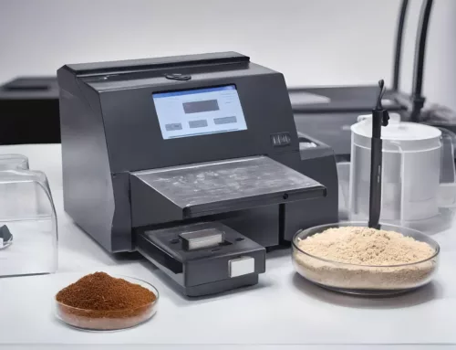
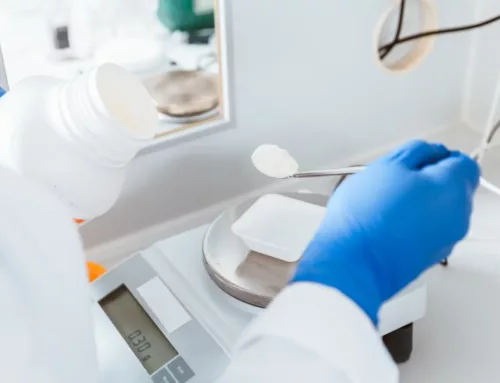
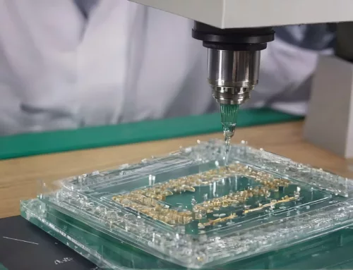
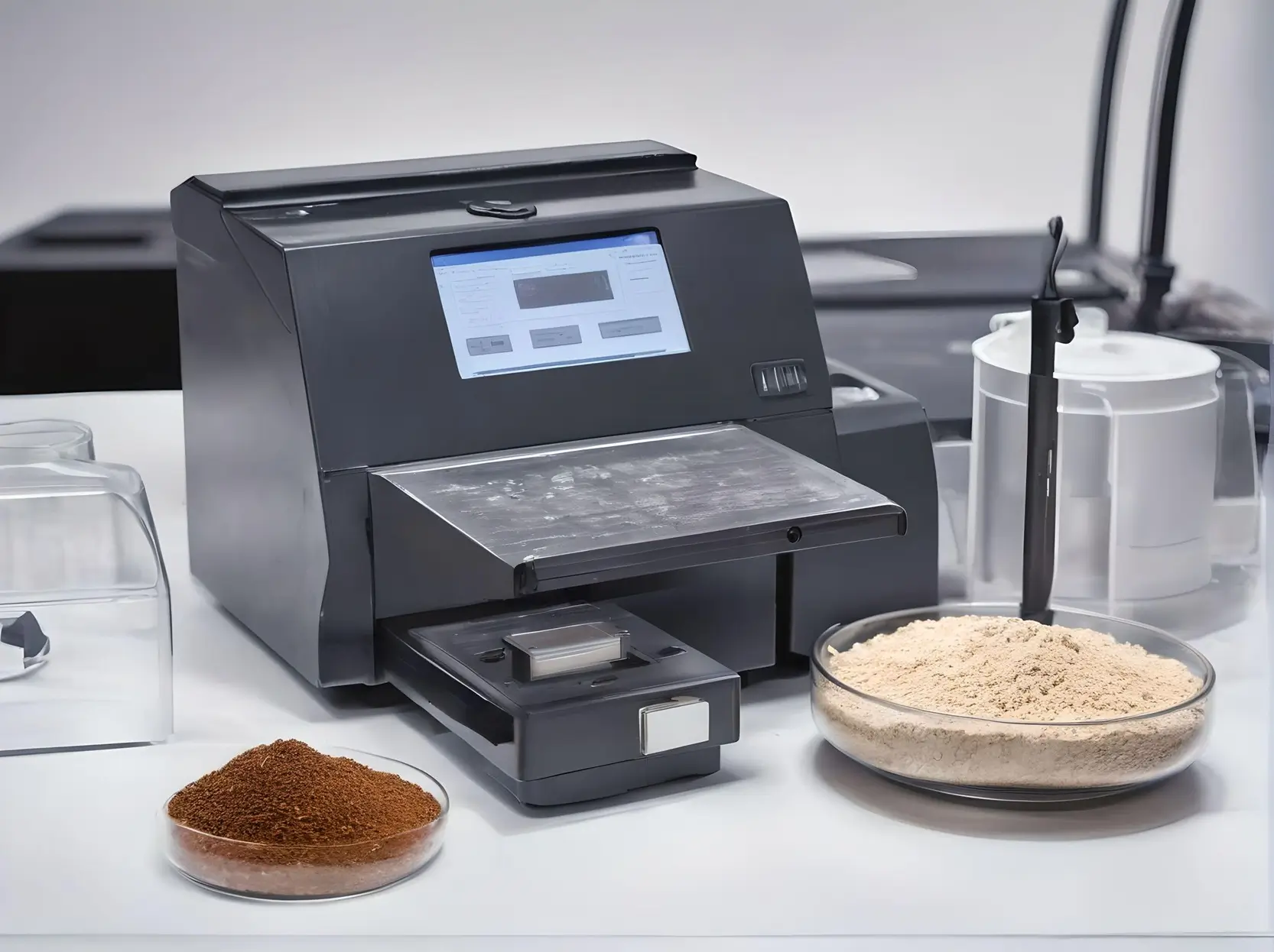
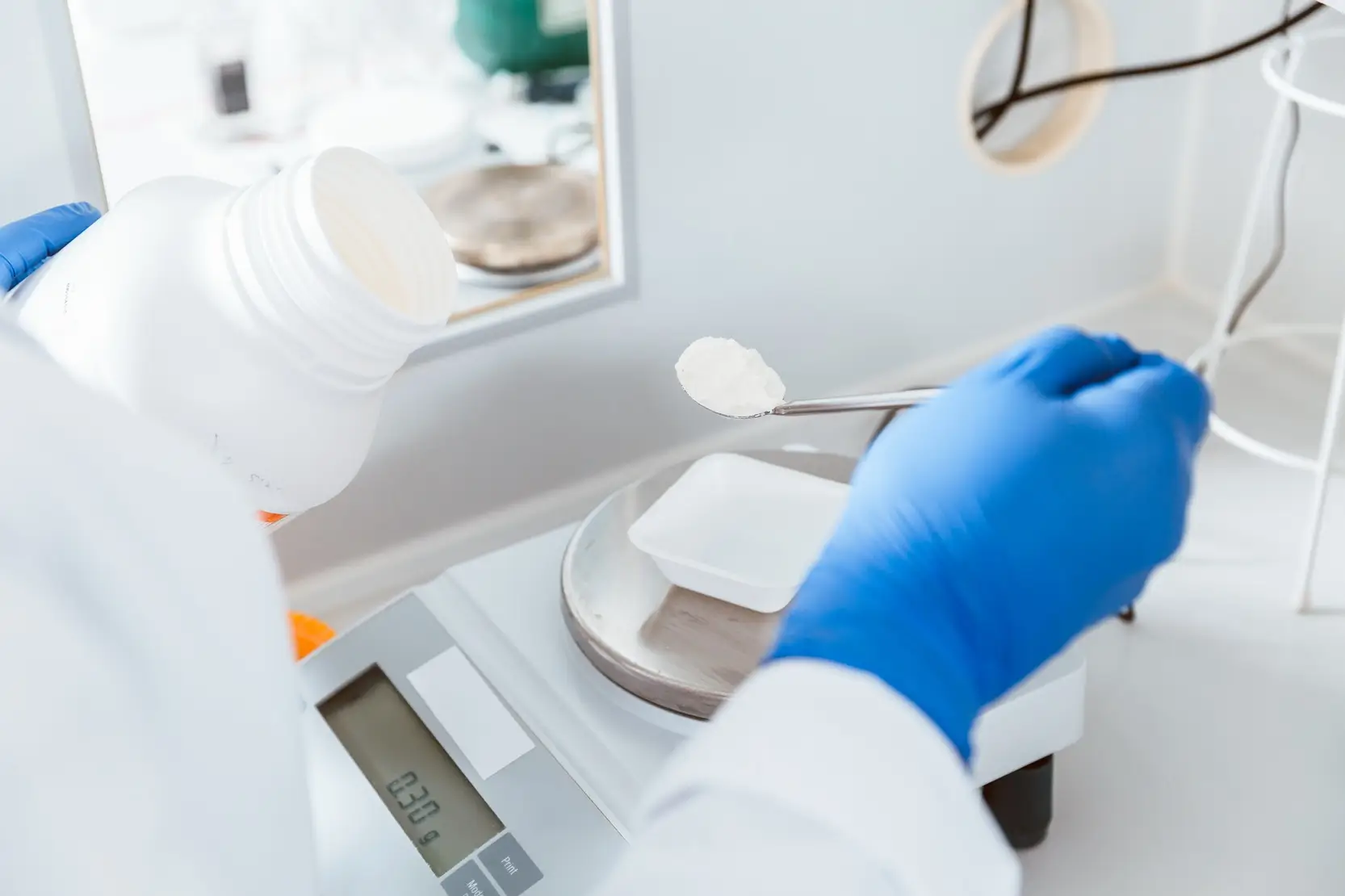
The fabrication of these microchips involves complex processes to create microfluidic channels, chambers, and sensors on a small scale. Photolithography is a foundational technique used to define the desired features on silicon or glass substrates, forming the basis of the microfluidic devices. Subsequent steps such as etching, deposition, and bonding are employed to create functional components and integrate additional layers or materials as needed. Powder technology also comes into play in various aspects of lab-on-a-chip fabrication. For example, powders may be used as precursor materials for thin-film deposition processes to create functional coatings or sensor layers on a microchip. Additionally, powder-based materials may be employed in additive manufacturing techniques to produce specialized components or structures within the microfluidic device.
Liquids and gases are other essential elements in the operation of lab-on-a-chip devices. Microfluidic channels and chambers for example are designed to manipulate liquid samples, reagents, and solvents with precision, enabling tasks such as sample transport, mixing, reaction, and detection. Gas-liquid interactions may also be utilized for processes such as bubble generation or droplet manipulation within the microfluidic system.
Lab-on-a-chip technology combines advancements in microfabrication, powder technology, liquids, and gases to create powerful analytical tools with applications in fields such as biomedical diagnostics, environmental monitoring, and drug discovery. As researchers continue to develop in these areas, lab-on-a-chip devices are set to change various aspects of scientific research and healthcare procedures.
Fabrication Process
The fabrication process of lab-on-a-chip devices is a multi-component process that involves precise engineering at the microscale to integrate complex analytical systems onto a single microchip. This process is significant as it enables the realization of the concept of lab-on-a-chip technology, which aims to miniaturize and automate laboratory processes for faster, more efficient, and cost-effective analysis of biological and chemical samples. At its core, the goal of lab-on-a-chip technology is to consolidate multiple laboratory functions, such as sample preparation,
analysis, and detection, onto a single chip-sized device. By doing so, researchers and practitioners can perform a wide range of analytical tasks using minimal sample volumes, reduced reagent consumption, and accelerated analysis times. The fabrication process starts with the selection of suitable substrate materials, such as silicon, glass, or polymers, which provide the foundation for constructing the microfluidic channels, chambers, and sensor components of the lab-on-a-chip device. Advanced microfabrication techniques, including photolithography, etching, deposition, and bonding, are then employed to create complex features and functional elements on the substrate.
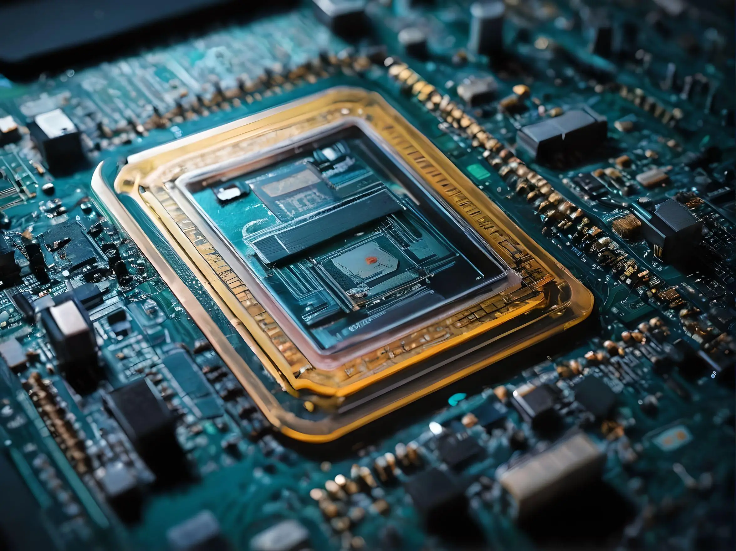
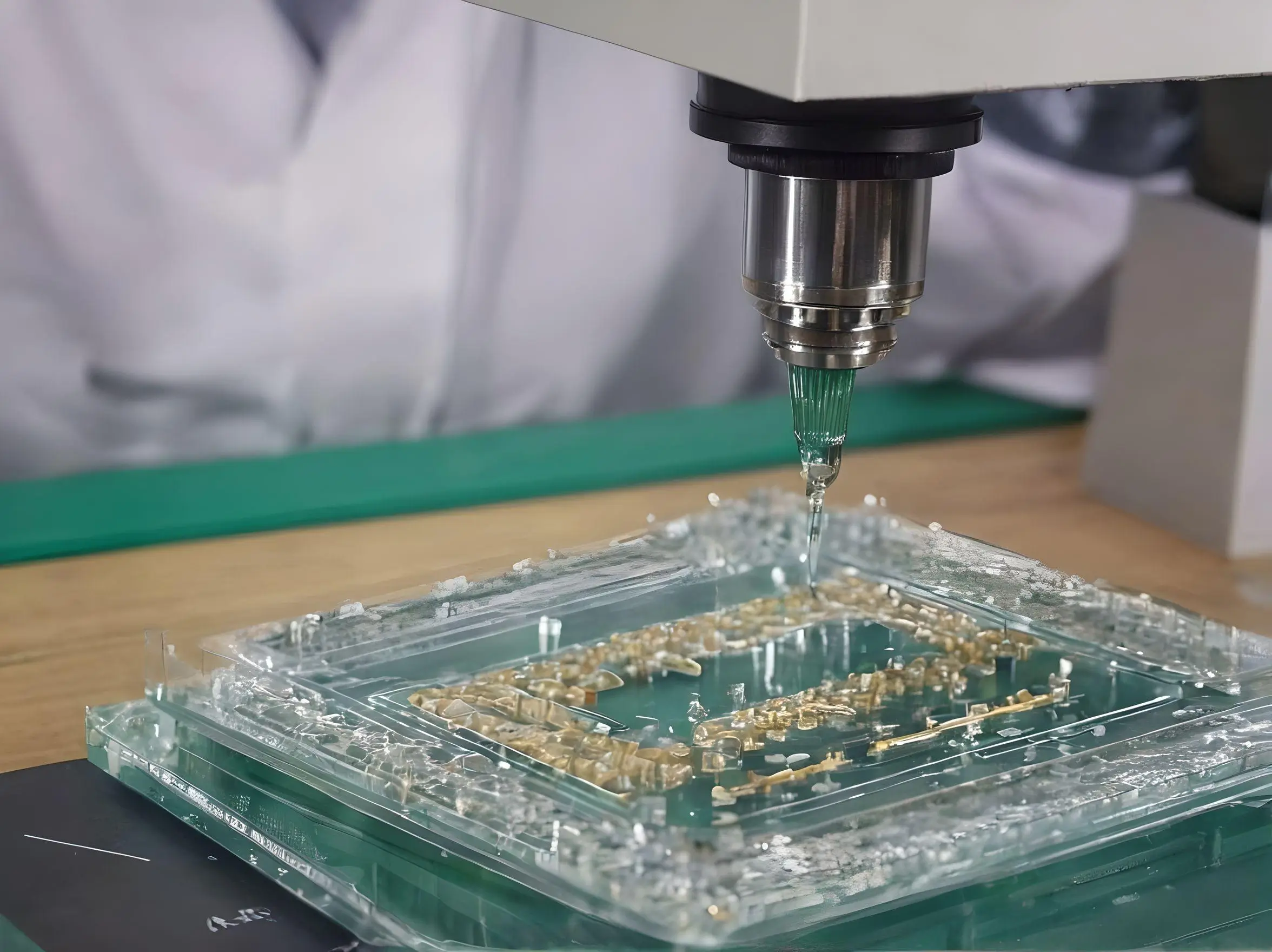
For instance, photolithography serves as a foundational technique for defining the desired patterns and structures on the substrate, allowing for precise control over the dimensions and geometries of microfluidic channels and chambers. Etching processes are utilized to transfer these patterns into the substrate, creating the physical features necessary for fluid manipulation and sample analysis. Deposition techniques, such as physical vapor deposition (PVD) or chemical vapor deposition (CVD), are used to coat the substrate with thin films of materials that serve as functional components, such as electrodes, sensors, or coatings for enhancing analytical capabilities. Bonding methods are
then used to seal multiple layers or substrates together, creating enclosed microfluidic channels and chambers that enable controlled sample manipulation and analysis.
The significance of this fabrication process lies in its ability to enable the integration of diverse analytical functions onto a single microchip, offering numerous benefits across various applications. By consolidating laboratory processes onto a chip-sized device, lab-on-a-chip technology facilitates portability, automation, and scalability, making it ideal for applications in fields such as biomedical diagnostics, environmental monitoring, drug discovery, and point-of-care testing.
Substrate Selection
The choice of substrate material is an important aspect of lab-on-a-chip fabrication, it directly impacts the performance, functionality, and compatibility of the resulting device. Substrates such as silicon, glass, and polymers each possess unique properties that must be carefully considered for the specific requirements of the intended application.
Silicon has long been a favored substrate material in microfabrication due to its excellent mechanical properties, thermal stability, and compatibility with semiconductor processing techniques. Silicon substrates offer high precision and uniformity, making them ideal for creating complex microstructures and features necessary for lab-on-a-chip devices. Additionally, silicon’s compatibility with photolithography, etching, and deposition processes enables precise patterning and integration of functional components. One of the key advantages of silicon substrates is their optical transparency in the infrared region, allowing for compatibility with various detection methods such as spectroscopy and imaging. This transparency enables real-time monitoring and analysis of biochemical reactions and cellular processes within microfluidic channels. However, silicon’s optical transparency diminishes in the visible spectrum, limiting its suitability for certain optical detection methods.
Furthermore, the rigidity of silicon substrates may pose challenges in certain applications where flexibility or biocompatibility is required. On the other hand, glass substrates offer excellent optical transparency across a wide range of wavelengths, making them well-suited for optical detection methods such as fluorescence spectroscopy and microscopy. Borosilicate glass, is commonly used, due to its low thermal expansion coefficient and chemical inertness, which ensure stability and compatibility with various sample types and reagents. Glass substrates also exhibit smooth surfaces and high flatness, facilitating precise patterning and bonding processes essential for lab-on-a-chip fabrication. Moreover, glass substrates can withstand high temperatures and harsh chemical environments, enhancing their versatility and durability in laboratory settings. However, glass substrates may be more brittle than other materials, increasing the risk of damage during handling or operation.
Additionally, their higher cost compared to polymers may limit their widespread adoption, particularly in disposable or low-cost applications.
Therefore polymers can offer several advantages over other materials in lab-on-a-chip fabrication, including low cost, flexibility, and ease of processing. Common polymers such as polydimethylsiloxane (PDMS), polymethyl methacrylate (PMMA), and cyclic olefin copolymer (COC) are frequently used due to their biocompatibility, transparency, and moldability.
PDMS, in particular, is widely used for its gas permeability, elasticity, and ease of fabrication using soft lithography techniques. PDMS-based devices are well-suited for biological applications, including cell culture, organ-on-a-chip systems, and point-of-care diagnostics. Polymers also offer advantages in terms of scalability and manufacturability, enabling mass production of disposable or single-use lab-on-a-chip devices at low cost.
However, polymers may exhibit higher levels of autofluorescence compared to glass or silicon substrates, which can interfere with the optical detection methods. The choice of substrate material therefore plays a critical role in determining the performance, functionality, and compatibility of lab-on-a-chip devices. Silicon substrates offer excellent mechanical properties and precision but may lack optical transparency in the visible spectrum. Glass substrates provide superior optical transparency and chemical inertness but may be more brittle and costly. Polymer substrates offer versatility, low cost, and ease of processing but may exhibit higher autofluorescence and lower thermal stability.
Coming up next
As we conclude this installment on lab-on-a-chip technology, it’s clear that the combination of microfluidics, materials science, and engineering has opened up more avenues of innovative solutions in various fields, from biomedical diagnostics to environmental monitoring and others. The fabrication process, with engineering at the microscale, enables the realization of lab-on-a-chip devices that can have a significant impact on scientific research and healthcare practices.
In the next part of our series, we will look into the fundamental principles and applications of photolithography, a key technique in the fabrication process of lab-on-a-chip devices. Photolithography plays a key role in defining microscale features and structures on substrate materials, enabling precise control over the layout and design of microfluidic channels, chambers, and sensor components.