

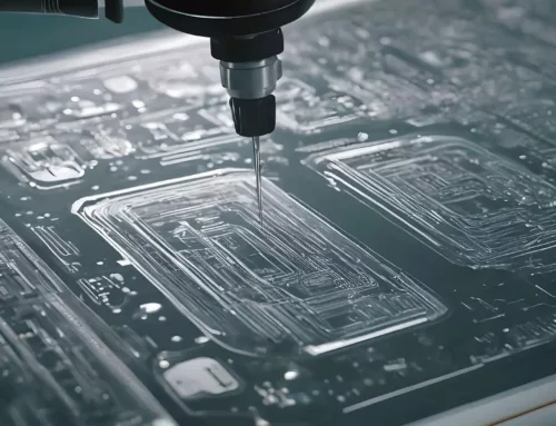
In the second series of lab-on-a-chip, we learned about photolithography, a fundamental technique used to fabricate lab-on-a-chip devices, to define complex microscale features on the substrate. In the third installment of our series, we look more into lab-on-a-chip fabrication by exploring thin-film deposition techniques. Thin-film deposition is key in enhancing the functionality and performance of lab-on-a-chip devices by enabling the precise coating of substrates with specialized materials.
Deposition Techniques
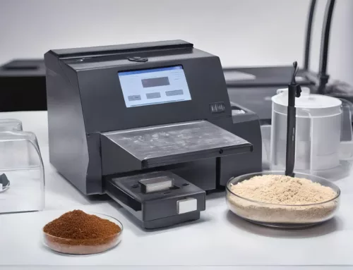
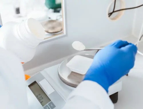
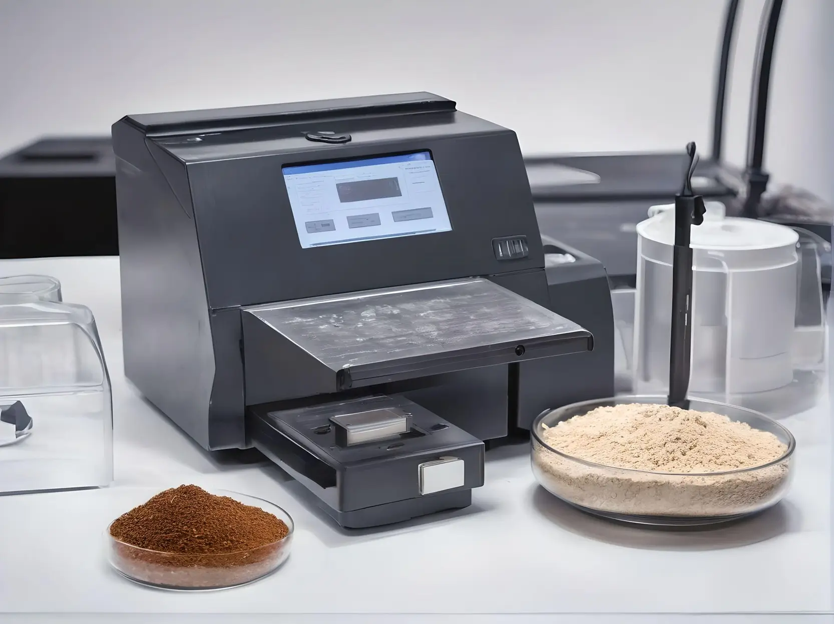
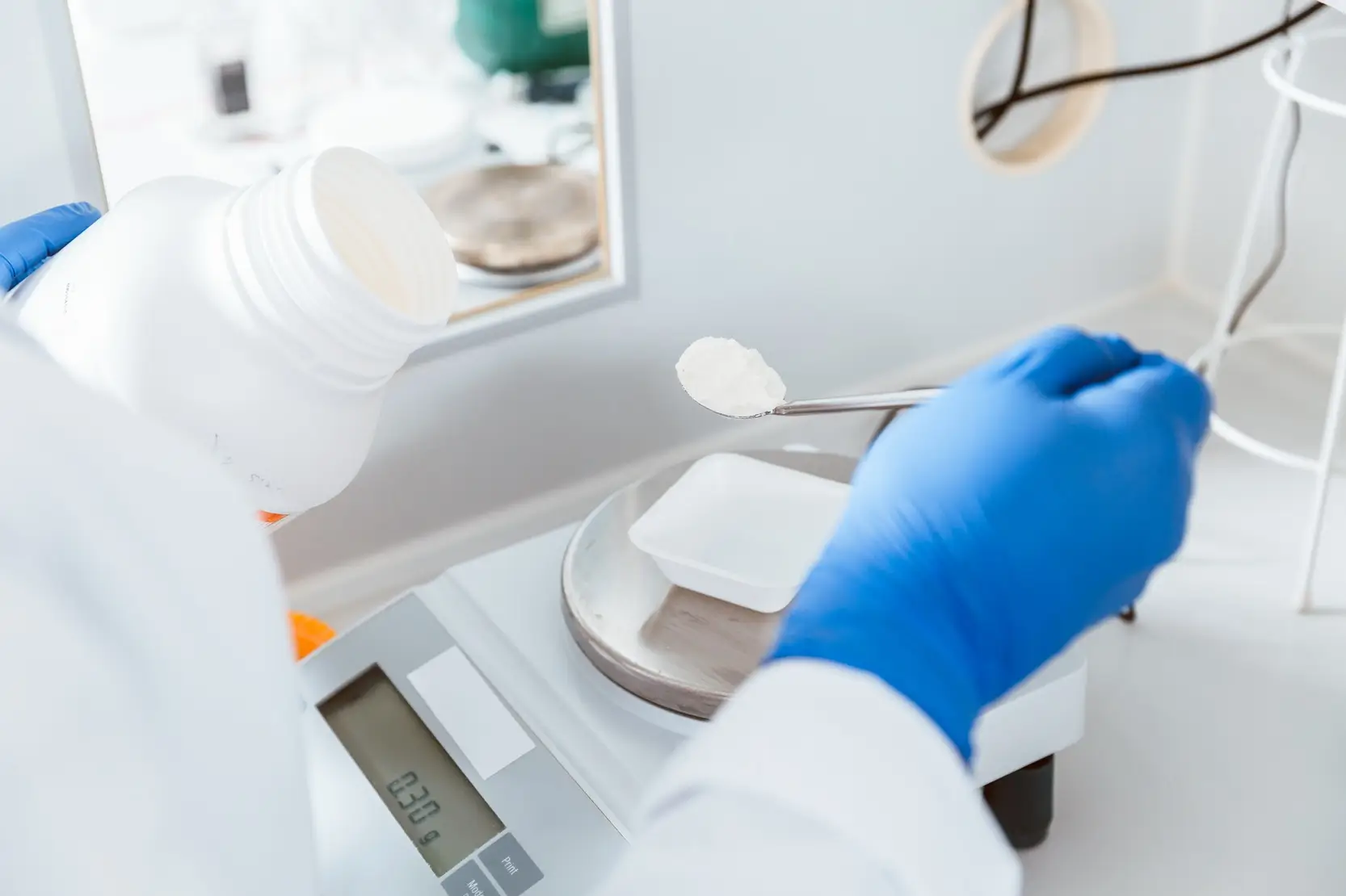
Depositing thin films of materials onto substrates is a key step in lab-on-a-chip fabrication, since it allows for the creation of functional layers essential for sensors, electrodes, coatings, and other components to adhere to. Two commonly used deposition techniques are physical vapor peposition (PVD) and chemical vapor deposition (CVD), each offering thier own unique advantages and capabilities. Physical vapor deposition for instance, involves the transfer of material from a solid source to the substrate in a vacuum environment, typically through processes such as evaporation or sputtering. During evaporation, the source material is heated to its melting point or higher, causing it to vaporize and condense onto the substrate surface. Sputtering, on the other hand, involves bombarding the source material with energetic ions, causing atoms or molecules to be ejected and deposited onto the substrate. Thin film deposition techniques PVD are widely used for depositing thin films of metals, semiconductors, and dielectric materials onto substrates with high precision and uniformity. PVD enables the creation of functional layers for sensors and electrodes, such as metal thin films for electrical contacts or sensing elements. PVD can also be used to apply protective or functional coatings onto the substrate surface, enhancing durability, biocompatibility, or chemical resistance.
On the other hand chemical vapor deposition techniques involve the deposition of thin films from chemical precursors in a gaseous state onto the substrate surface. The precursor molecules react or decompose on the substrate surface, forming a solid film through chemical reactions or vapor-phase condensation.
CVD processes can be categorized into several subtypes, including thermal CVD, plasma-enhanced CVD (PECVD), and atomic layer deposition (ALD), each offering unique advantages and control over film properties. CVD techniques are used to deposit a wide range of materials, including metals, oxides, nitrides, and polymers, onto substrates with precise control over film thickness and composition.
CVD is utilized to create functional layers for lab-on-a-chip devices, such as insulating or passivating layers, dielectric films, or surface modification coatings. CVD enables the integration of sensing materials, such as metal oxide thin films for gas sensors or biosensing surfaces for biomolecular detection, onto the substrate surface.
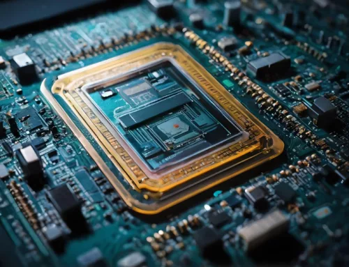
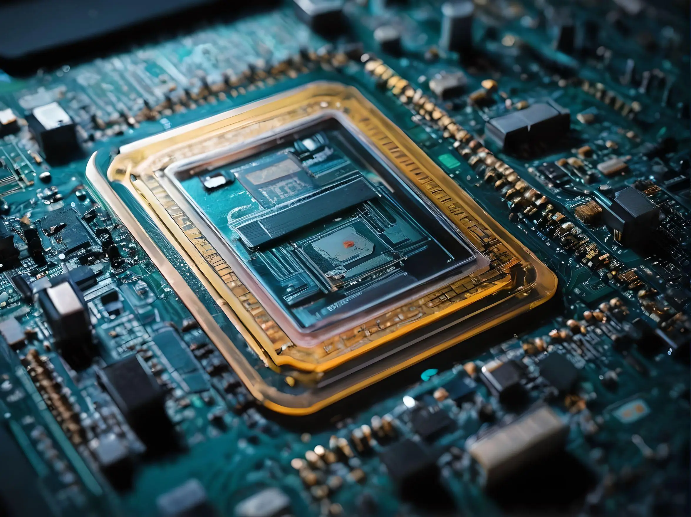
Thin film deposition is a decisive step in lab-on-a-chip fabrication, as it enables materials to adhere to the substrate, forming functional layers crucial for sensors, electrodes, coatings, and other components.
These thin films serve various purposes, including providing electrical conductivity for electrodes, enhancing sensitivity and selectivity for sensors, and protecting the substrate from chemical or biological interactions. For example, in electrochemical biosensors, thin films of noble metals (e.g., gold or platinum) deposited via PVD techniques serve as electrodes for detecting biomolecular interactions. In gas sensors, metal oxide thin films deposited using CVD processes provide high surface area and sensitivity for detecting target analytes. Furthermore, deposition techniques allow for the integration of multiple functional layers onto a single substrate, enabling the development of complex lab-on-a-chip devices with integrated sensing, actuation, and analysis capabilities.
Bonding and Sealing
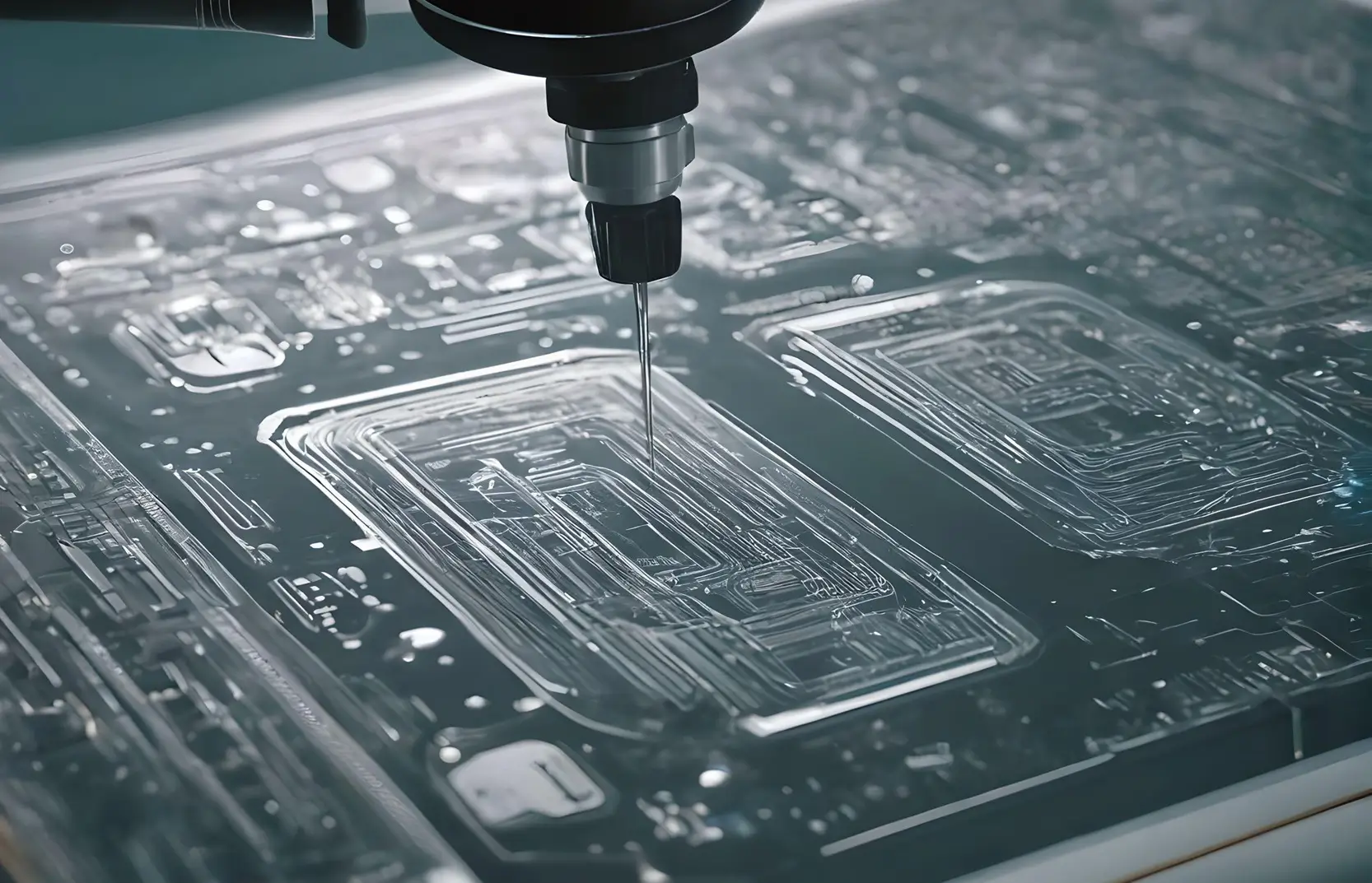
Bonding methods are essential for sealing multiple layers or substrates together to form enclosed microfluidic channels and chambers in lab-on-a-chip devices. Various bonding techniques, including thermal bonding, adhesive bonding, and plasma bonding, are utilized to achieve leak-free seals and ensure reliable operation.
Thermal bonding, also known as thermal fusion bonding or thermal compression bonding, involves applying heat and pressure to two or more substrates to create a permanent bond at the interface. This bonding method is commonly used for bonding thermoplastic materials such as polymethyl methacrylate (PMMA) or cyclic olefin copolymer (COC). Prior to the bonding process, the substrate surfaces are typically activated using methods such as plasma treatment or corona discharge treatment to enhance adhesion. The substrates are heated to a temperature close to or slightly above their glass transition temperature (Tg) or melting point, depending on the material, and then pressed together under controlled pressure. After bonding, the assembled and pressed structure is allowed to cool and solidify, forming a strong and post-exposure bake permanent bond at the interface.
The thermal bonding ensures intimate contact between substrate surfaces, resulting in leak-free seals essential for reliable fluidic operation.The bonding process also creates a strong intermolecular interactions between the substrate molecules, leading to a high bond strength and mechanical stability. The thermal bonding also allows compatibility with microfabrication techniques and for the integration of complex features such as channels, chambers, and electrodes within the bonded structure.
Another technique used is adhesive bonding which involves the use of adhesives or bonding agents to bond two or more substrates together. Adhesive bonding techniques offer flexibility in material selection and bonding conditions, making them suitable for bonding diverse materials such as glass, polymers, and metals. Similar to thermal bonding the substrate surfaces need to be cleaned and treated to ensure proper adhesion of the adhesive. The adhesive is applied to one or both substrate surfaces using methods such as dispensing, spraying, or spin-coating. The substrates are aligned and pressed together, and the adhesive is allowed to cure or polymerize under controlled conditions such as temperature, pressure, and curing time. The versatility of adhesive bonding
allows for bonding of diverse materials, including materials with different coefficients of thermal expansion or surface energies. Adhesives can also fill gaps and irregularities at the substrate interface, providing conformal sealing and enhancing bond strength and some adhesive formulations enable bonding at room temperature, eliminating the need for high-temperature processing and reducing thermal stress on delicate components.
Another innovative technique is plasma bonding, also known as plasma-assisted bonding or plasma activation bonding, involves the use of plasma treatment to modify substrate surfaces and promote adhesion at the interface.
This bonding method is particularly effective for bonding materials with low surface energy or inert surfaces. To prepare, the substrate surfaces are exposed to a low-pressure plasma environment, typically consisting of reactive gases such as oxygen, nitrogen, or hydrogen. This surface activation modifies the surface chemistry and topography of the substrates, creating reactive functional groups and or increasing the surface energy. After the plasma treatment, the substrates are aligned and pressed together to form a bond. The reactive surface groups facilitate bonding by promoting
intermolecular interactions between substrate molecules which enhances surface wettability and adhesion, promoting strong bonds between substrate materials. The plasma treatment can be tailored to specific materials and bonding conditions, allowing for selective surface modification without affecting bulk properties. For examole, plasma bonding can be performed at relatively low temperatures, minimizing thermal stress on sensitive components and enabling bonding of heat-sensitive materials.
Critical in all processing techniques mentioned are leak-free seals to ensure reliable fluidic operation in lab-on-a-chip devices. Any leakage or seepage along the bonded interface can compromise the functionality and accuracy of the device, leading to unreliable results and potential sample contamination. Therefore, choosing the appropriate bonding method and optimizing bonding parameters are essential for achieving leak-free seals and ensuring the performance and longevity of lab-on-a-chip devices in various applications.
Mastering Desposition
In conclusion, mastering deposition techniques and bonding methods is crucial in lab-on-a-chip fabrication. These processes enable the creation of functional layers and leak-free seals essential for device performance and reliability. Moving forward, our next focus will be on “Functional Component Integration,” where we’ll delve into how sensors, electrodes, and actuators are seamlessly integrated into lab-on-a-chip devices to unlock their full potential for scientific and medical applications.
The next installment will introduce the methods and benefits of functional component integration, as we go deeper into the process of seamlessly incorporating sensors, electrodes, and actuators into lab-on-a-chip devices. This critical step unlocks the full potential of these devices for various scientific and medical applications.