Lab-on-a-Chip fabrication: 
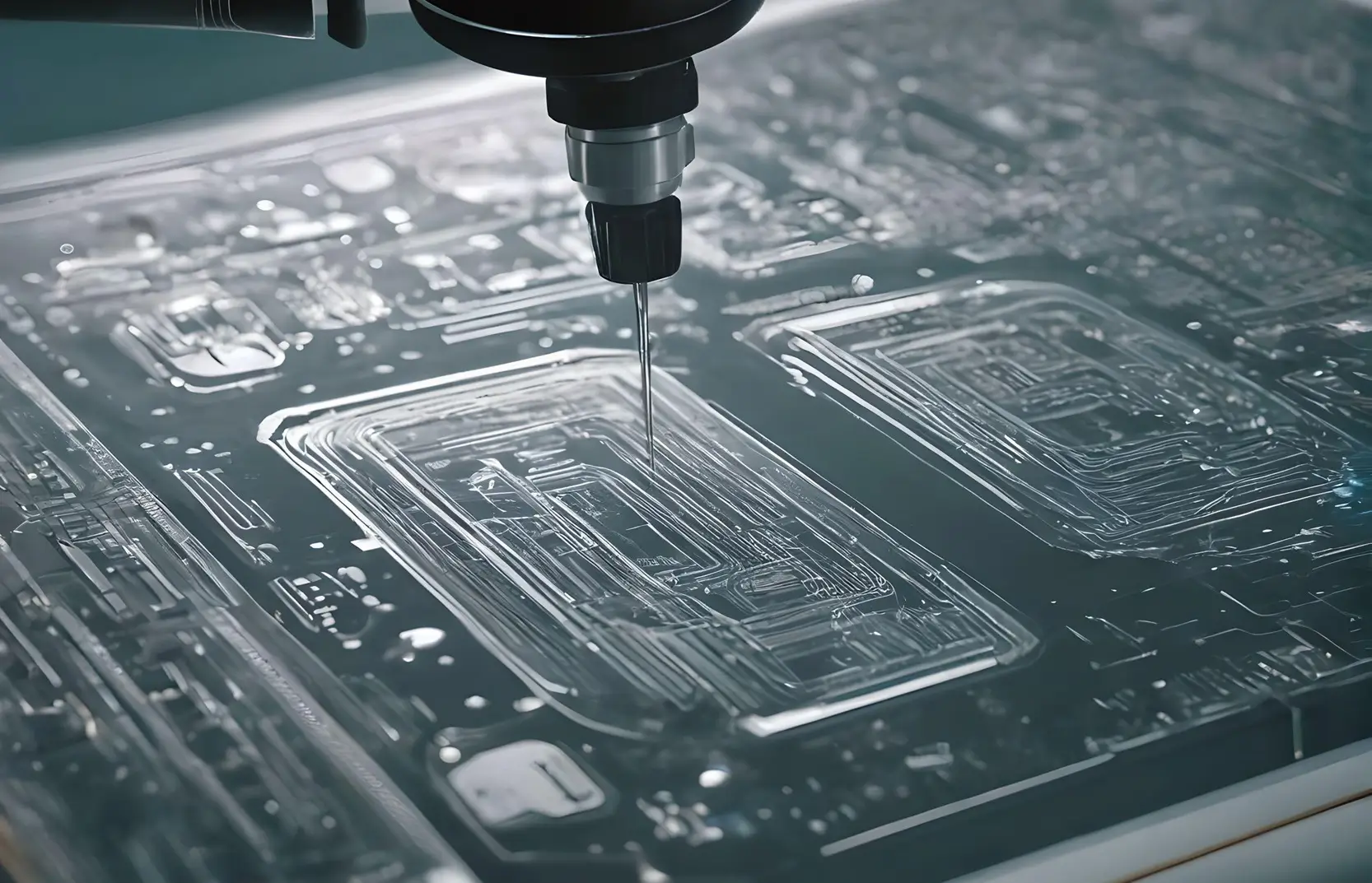
The Power of Photolithography and Etching Technologies - Part 2 article

In the first part of our series on lab-on-a-chip technology, we looked into various scientific disciplines, including microfluidics, materials science, chemistry, and engineering, that have led to the development of the lab-on-a-chip analytical approach. The article gave a perspective on how advancements in microfabrication techniques, particularly photolithography and thin-film deposition, have enabled precise manipulation of fluids and materials at the microscale. To continue we will look deeper at what photolithography entails when it comes to lab on a chip fabrication.

Photolithography

Photolithography is a fundamental technique used in the fabrication of lab-on-a-chip devices to define complex microscale features on the substrate. This process involves patterning photoresist layers on the substrate using masks and UV light exposure. Below, we provide a detailed perspective of the photolithography process, highlighting the steps of coating, exposure, development, and post-exposure bake, and emphasizing the precision required to define microscale features. Before the photolithography process begins, the substrate (typically silicon, glass, or polymer) is cleaned thoroughly to remove contaminants and ensure proper adhesion of subsequent layers. This step is important in achieving a uniform coating and accurate patterning of the photoresist.

The substrate is spin-coated with a layer of photoresist, a light-sensitive material that undergoes chemical changes upon exposure to UV light. The thickness of the photoresist layer is carefully controlled to achieve the desired feature dimensions in the final device. Spin-coating ensures uniform coverage of the substrate surface, which is essential for precise patterning.
A photomask containing the desired pattern is aligned with the coated substrate using specialized alignment tools and equipment. The photomask consists of opaque regions that block UV light and transparent regions that allow UV light to pass through, creating the desired pattern on the photoresist layer. The substrate is then exposed to UV light, which selectively activates the photoresist in the exposed areas while leaving the unexposed areas unaffected.

After exposure, the substrate is immersed in a developer solution that removes the unexposed regions of the photoresist, leaving behind the patterned photoresist layer.
The development process is carefully controlled to ensure the complete removal of the unexposed photoresist while preserving the patterned features with high fidelity. Proper development is critical for achieving accurate and reproducible microscale features.

Following this development, the substrate undergoes a post-exposure bake process to further stabilize the patterned photoresist layer and enhance its adhesion to the substrate. This step involves heating the substrate at a specific temperature for a predetermined duration, allowing the photoresist to crosslink and harden.

The post-exposure bake step is needed to improve the durability and reliability of the patterned features, particularly in subsequent processing steps such as etching or deposition. The photolithography process requires a high level of precision and control to achieve microscale features with sub-micron resolution.

Factors such as photoresist thickness, exposure dose, and development time must be carefully optimized to ensure accurate pattern transfer from the photomask to the substrate. Additionally, the alignment of the photomask with respect to the substrate has to be precise to avoid misalignment errors that will compromise the integrity of the final device.

Overall, photolithography is an essential step in the fabrication of lab-on-a-chip devices, enabling the precise definition of microscale features necessary for fluidic channels, chambers, electrodes, and other functional components. By carefully controlling each aspect of the photolithography process, researchers can achieve high-quality patterns with exceptional accuracy and reproducibility, laying the foundation for the development of advanced microfluidic systems for a wide range of scientific and medical applications.

Etching

Etching techniques also play an essential role in transferring patterns from the photoresist layer to the substrate, defining the desired channel geometries and depths in lab-on-a-chip devices. Common etching methods include wet etching and dry etching, each offering unique advantages and control over the etching process. Wet etching for example involves the selective removal of material from the substrate using chemical etchants in liquid form. The choice of etchant and etching conditions depends on the substrate material and desired etch rate. Common etchants used in wet etching include acids, bases, or solvents that react with the substrate material to dissolve or dislodge it selectively. The choice of etchant also determines the selectivity and etch rate of the process. Different etchants exhibit varying degrees of selectivity towards different materials, allowing for precise control over the etching process. Etching temperature affects the etch rate and selectivity of the process. Higher temperatures typically result in faster etch rates but may also increase the risk of non-uniform etching or damage to the photoresist layer. The duration of the etching process determines the depth of the channels or features. The careful control of etch time is important in achieving the desired channel geometries and depths without over-etching or

under-etching. Dry etching, also known as plasma etching, also involves the removal of material from the substrate, however, reactive ions or gases in a plasma environment are used instead liquid etchants. Dry etching techniques offer higher precision, selectivity, and control over the etching process compared to wet etching. Common dry etching methods include reactive ion etching (RIE), inductively coupled plasma (ICP) etching, and deep reactive ion etching (DRIE). The Control of the dry etching parameters relies on selecting the appropriate process gases, as their composition significantly impacts the etch rate, the selectivity, and sidewall profile of the patterns being etched into the material. Reactive gases such as fluorine-based or chlorine-based compounds react with the substrate material to form volatile byproducts, which are then removed from the surface. The power applied to the plasma source affects the density and energy of the ions bombarding the substrate surface. Higher plasma power typically results in faster etch rates but may also increase the risk of sidewall damage or roughening. The pressure within the etching chamber controls the density and distribution of reactive species in the plasma, therefore optimal pressure conditions are necessary to achieve uniform etching across the substrate surface and minimize sidewall roughness.

Both wet etching and dry etching techniques offer precise control over channel geometries and depths in lab-on-a-chip devices. By carefully selecting etchants or process gases, controlling etching parameters such as temperature, time, plasma power, and pressure, researchers can achieve the desired channel dimensions, aspect ratios, and surface roughness. For example, wet etching may be preferred for shallow channels with smooth sidewalls, while dry etching techniques offer superior control over feature dimensions and aspect ratios, making them suitable for deeper and high-aspect-ratio structures. Additionally, advanced techniques such as deep reactive ion etching (DRIE) enable the fabrication of deep, vertical features with high aspect ratios, essential for applications such as microfluidic channels and through-silicon vias (TSVs).

Finally by choosing the desired etchants or process gases and optimizing the etching parameters, researchers can achieve the desired channel geometries and depths required for various microfluidic applications, advancing the development of next-generation lab-on-a-chip devices for scientific and medical research.

In this series segment, we talked about the process of photolithography, which can be seen as a key cornerstone in the fabrication of microscale features essential for fluidic channels, chambers, electrodes, and other functional components. Photolithography also empowers researchers with the precision needed to define microstructures crucial for the operation of lab-on-a-chip devices, revolutionizing scientific research and healthcare practices. In the next part of our series, we will explore another vital aspect of lab-on-a-chip fabrication: thin-film deposition. Thin-film deposition plays an important role in enhancing the functionality and performance of lab-on-a-chip devices by coating substrates with specialized materials to create electrodes, sensors, or functional coatings.

Conclusion